
Bit Timing Calculation
Abbreviations used: tNBT - Nominal CAN Bit time tsyn - Syncronization segment PD - Propagation delay tseg1 - Time segment 1 tseg2 - Time segment 2 tq - Time quantum BRP - Baud rate prescaler fsys - Controller system clock fclk - Clock Frequency NBT - Number of tq in tNBT tPD - Propagation Delay time
The CAN protocol supports bit rates in the range of 1Kbps and 1000Kbps. Each node has its own clock generator and oscillator.
Configuring the bit timing parameters for each node can facilitate a common bit rate on the bus.
The Nominal CAN Bit Time (NBT) divided into four segments as shown below.
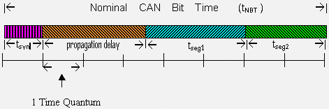
Hence, tNBT = tsyn + tPD + tseg1 + tseg2
The Nominal Bit Rate is the number of bits per second.
Nominal Bit Rate = 1 / Nominal Bit Time
Each segment consists of a specific programmable number of time quantum, which is basic unit of bit time. The synchronization segment is that part of the bit time where the edges of the CAN bus level.
Mapping between fsys and tq: The controller needs to regulate its system clock period (1 / fsys) in order to realise the time quantum (tq) desired. The coefficient of regulation is defined as Baud Rate Prescaler (BRP). Hence,
tq = 2 * (BRP/ fsys ) (I)
fsys = fclk / 2 (II), where fclk is Clock Frequency
tNBT = 1 / baud rate (III)
NBT = tNBT / tq (IV)
Hence from equation (I), (II) and (III)
NBT = ( 1 / baud rate ) / (4 x BRP/ fclk)
=> NBT x BRP = fclk / (4 X Baud Rate)
The product value NBT x BRP will be an integer value. Appropriate baud rate will be calculated to get an integer value for the above product. This will ensure that Clock Frequency remains same for a particular CAN controller.
Additionally,
NBT x tq = tNBT = tsyn + tPD + tseg1 + tseg2 (V)
Clearly,
tsyn = tq (VI)
tseg1 = TSEG1 x tq (VII)
tseg2 = TSEG2 x tq (VIII)
tPD = PD x tq (IX)
Therefore from equation (VI), (VII) and (VIII).
NBT = TSEG1 + TSEG2 + PD + 1.
Sampling Point = ((NBT - TSEG2) / NBT) x 100 %.
The neoVI hardware consist of three registers namely CNF1, CNF2, CNF3 the details of which are given below:
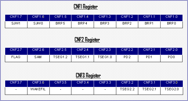
SAM (Sampling) = 0 or 1 (1 or 3)
SJW = 2 x SJW1 + SJW0 + 1
BRP = 32 x BRP5 + 16 x BRP4 + 8 x BRP3 + 4 x BRP2 + 2 x BRP1 + BRP0 + 1
TSEG1 = 4 x TSEG1.2 + 2 x TSEG1.1 + TSEG1.0 + 1
TSEG2 = 4 x TSEG2.2 + 2 x TSEG2.1 + TSEG2.0 + 1
FLAG = 0 or 1 ( “TSEG2 Ignored” or “TSEG2 Considered”)
Authoritative source: BUSMASTER DITA help source bit_timing.dita, compiled into BUSMASTER.CHM with the application.